Page 14 of 27
Posted: 09 Jun 2016, 11:45
by mohitgarg
matt3o wrote: honestly depends mostly on pricing
Maybe ask your manufacturer if they charge differently for 1.2mm PCB vs 1.6mm, if yes, how much are we looking at for a 18*38mm PCB (Estimated size)
Posted: 09 Jun 2016, 11:59
by matt3o
mohitgarg wrote: matt3o wrote: honestly depends mostly on pricing
Maybe ask your manufacturer if they charge differently for 1.2mm PCB vs 1.6mm, if yes, how much are we looking at for a 18*38mm PCB (Estimated size)
how many components?
Posted: 09 Jun 2016, 23:20
by bpiphany
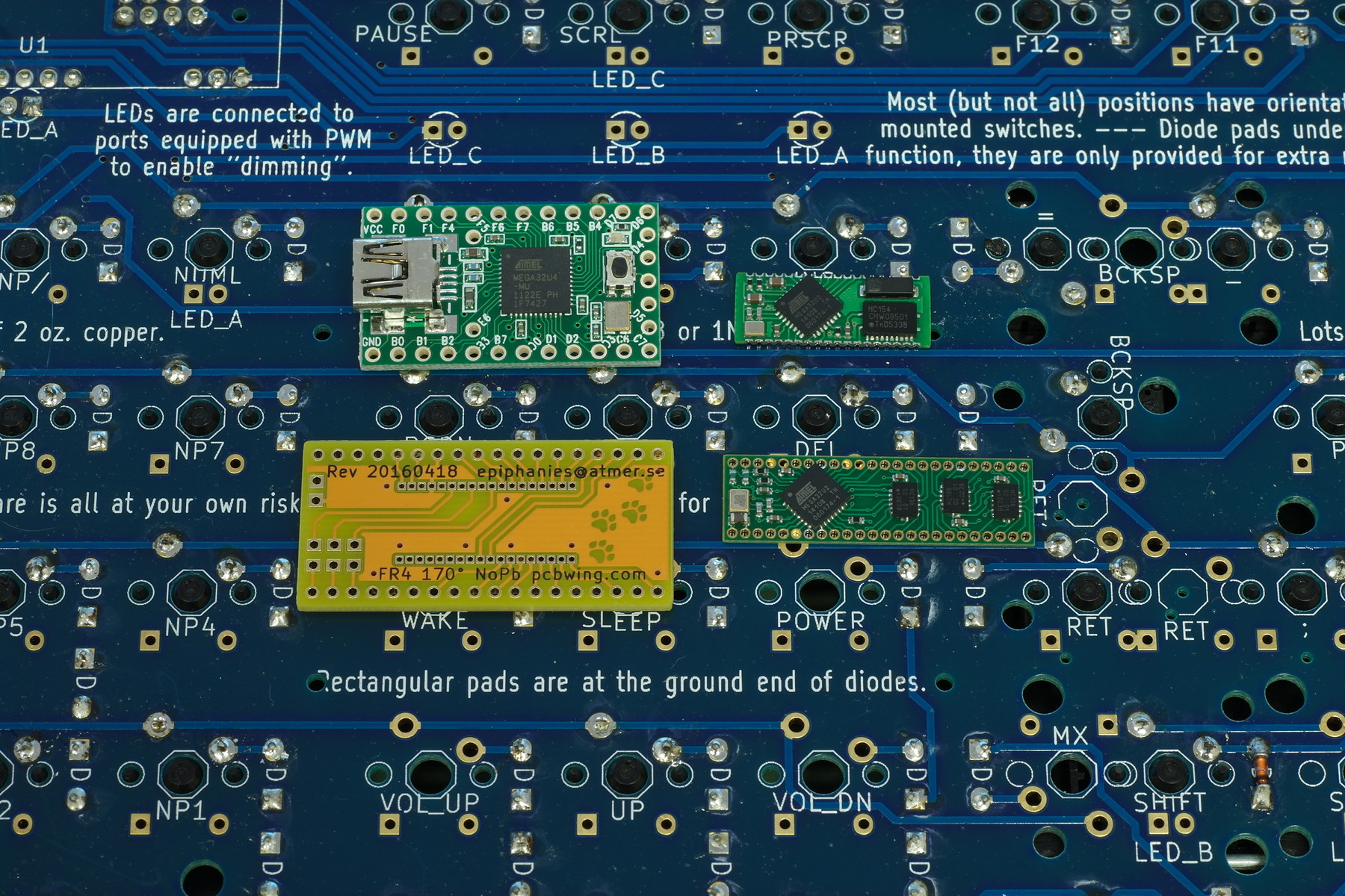
That Kimera looks pretty big still.. Is there any schematic for it? And isn't that a resonator? I didn't think it would run USB very well without the accuracy of a crystal or oscillator.
Why not go small, and I mean small, if you're looking at QFNs anyway? (Perhaps the ARMs don't come in anything larger?). Component wise I figure it's about the same. The ARM might not need an oscillator, on the other hand you need a regulator (which you can benefit from for other functions as well, like Bluetooth modules).
The yellow board is there only because it happens to be pretty much exactly 18x38mm. The photo lies a
tiny bit, the Teensy is angled more towards the camera, and may look a bit wider. And I would recommend sticking to 0.05" in place of 1mm pitch... Anyone capable of soldering SMD should be able to solder 1.27mm pitch =)
- controllers.jpg (648.44 KiB) Viewed 8660 times
Edit: Found the
schematic. I don't think I get the idea. Sure it's neat with IO-expanders, but they just threw 11 perfectly good ATmega GPIOs away... And that sure is a resonator.
Posted: 10 Jun 2016, 00:37
by Matt_
The point of this controller is not to be the smallest size possible, but to be easy to add to any DIY project, and since it is intended to be sold assembled nobody is expected to know how to solder QFNs

0.1" headers will probably be easier for everyone to work with.
Posted: 10 Jun 2016, 08:27
by bpiphany
But still.. Make it narrow enough to fit between a row of switches. 0.1" pitch will just make it very long... And I really think 0.05" should be solderable by most people. And I would stick to a separate USB connector, and separate multiplexers. Make stuff fit between switches. All that's of course just my 50¢, this isn't my project =)
Posted: 10 Jun 2016, 09:39
by matt3o
it's about flexibility more than size.
why making is super tiny when a bigger board can adapt to more use cases? you can place it directly under two switches, that is a great thing for hand-wired keyboards. if you don't want to do that it's still thin enough to be placed between the plate and the PCB. if you don't want to do that either you can add some headers and place it basically anywhere you want. you can use directly the onboard USB or route an extension cable.
I don't think size really matters here, because --for example-- with a super tiny board it wouldn't be possible to use the onboard usb.
Posted: 10 Jun 2016, 15:07
by MrBishop
ive been looking for something similar to this to integrate into future projects big and small. i was looking at the AT90USB1286 thats on board the Teesny2++. would be cool to be able to build a 40% or a 100% board using a similar controller even if some of the pins are not used. simplifying the design with a cookie cutter logic controller base configuration hardware side. it would also be nice to be able to drop this same schematic onto a daughter board allowing more flexibility in prototyping or testing. basically making a teensy 2 and 2++ killer in one. very much like bpiphany made if not exactly what he made

Posted: 21 Jun 2016, 11:54
by mohitgarg
So we good good for 1.2mmPCB with USB Type-C?
Posted: 21 Jun 2016, 17:22
by matt3o
I would be good with a PS/2 connector at this point

just let's have this finalized!
Posted: 30 Jun 2016, 10:16
by pomk
Just a note that if routing seems difficult with the switch holes present, we can probably route with 4 mil traces and produce via PCBway. The per piece price at 100 pcs is just 90 cents, which is just a bit over double the price compared to 6mil. (4mil traces, 0,2mm drill vs. 6mil, 0,3mm drill)
4 layers with 4mil would also give the option of using the BGA model of the same chip, this would raise the price per PCB to 1,5 dollars, but would allow for practically any layout. Even both switch positions both for mx and alps as well as mx leds.
Posted: 30 Jun 2016, 11:26
by mohitgarg
Definitely options to consider.
Regarding the delay, on my side it's purely because of lack of time, I have been busy and disturbed due to work for the last couple of weeks. Also been having a generally bad run of luck of late in life.
Posted: 11 Jul 2016, 10:37
by hasu
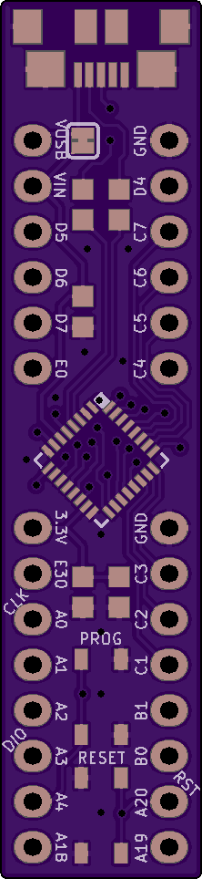
I designed this breakout pcb for KL27Z(32QFN) which is 300mil width, having breadboard prototyping in mind. The width is very tight spacing, without placing vias beneath the chip(thermal pad) I couldn't draw traces enough.
I ordered it from OSHpark and will see if it works, in particular tented vias under thermla pad.
Posted: 11 Jul 2016, 10:52
by matt3o
lovely board hasu! I wish I could design them
Posted: 24 Aug 2016, 12:14
by matt3o
Posted: 25 Aug 2016, 02:34
by pomk
I should have time next Tuesday to get this done.
Posted: 06 Sep 2016, 22:34
by regack
I'm a little late to the party, but I've had a great time reading through the thread. I remember that mini QFN controller that bpiphiany made a few years ago, I found it inspiring - I was hoping a community created controller would take over for the Teensy 2.0 in the following years but now it's finally moving in that direction.
I like the idea of integrating the two switches into the PCB, they could become part of the matrix for hand-wired boards (as long as all of the possible footprints are there). Whenever the controller footprint gets finalized, I'd be happy to contribute to making a board that can take advantage of it.
Posted: 07 Sep 2016, 03:46
by hasu
hasu wrote: I designed this breakout pcb for KL27Z(32QFN) which is 300mil width, having breadboard prototyping in mind. The width is very tight spacing, without placing vias beneath the chip(thermal pad) I couldn't draw traces enough.
I ordered it from OSHpark and will see if it works, in particular tented vias under thermla pad.
I had two critical mistakes on the board, reverse USB signal lines and misalignment of pins

completely disaster. Yesterday, palced order new pcb and stencil to easyeda.

Not use it in real application yet and have to work on its bootloader and flash tool.
Posted: 07 Sep 2016, 14:58
by regack
hasu wrote:
I had two critical mistakes on the board, reverse USB signal lines and misalignment of
pins
completely disaster. Yesterday, palced order new pcb and stencil to easyeda.
Not use it in real application yet and have to work on its bootloader and flash tool.
I really like the format/shape though, so it's still useful learning, even if you lost some time and the cost of a few components. Is the pin alignment problem that the pins do not align with a breadboard?
---
Anyone up for the idea of settling on a common mechanical design which can support multiple MCUs? Obviously not on the exact same PCB, but a common physical layout with important pins always in the same place (e.g. VUSB, USB d+, USB d-, Vcc, Gnd, reset, miso, mosi, clk, SWDIO, SWCLK etc).
It could have a baseline profile that can also be extended to account for size varaitions (e.g. 38.1mm x 18mm base --> 57.15mm x 18mm extended) - usb placement remains per the spec.
The Elf could be one such implementation, bpiphany could design one using decoders, etc... I'm not trying to derail anything, just leaning towards creating a platform that can be used for the next 5-10 years as the Teensy seems to have done.
In that regard, I'd lean towards USB-C even though I don't own any USB-C right now - of course, cost has to be taken into account.
Posted: 13 Sep 2016, 19:14
by matt3o
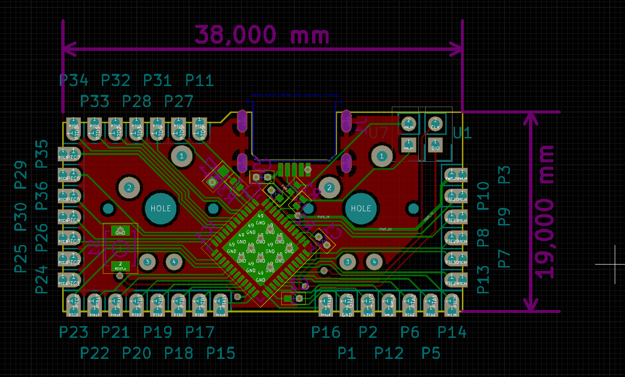
A new benefactor (who is not keen to participate to the forum discussion) worked on this.
Any comments, suggestions, thoughts?


Posted: 13 Sep 2016, 23:35
by pomk
The routing seems good for the parts that he has done already, but:
1. It wont stay stable on two switches if they are not soldered on to the pcb. - Needs solder pads at least on the bottom side.
2. No led support, even if it was soldered on a pcb. - Needs holes and maybe pads too.
3. No mid mount connector making it a bit thick. - Just a personal preference.
4. No usb type c. - Just a personal preference.
5. What is the deal with the crystals and some additional ICs on board? I thought they are not needed with the previously selected IC.
Posted: 14 Sep 2016, 08:07
by matt3o
yup the additional crystal is not needed and will be removed. padding on the switch holes is not strictly needed but let's see if we can fit it.
Posted: 14 Sep 2016, 10:35
by pomk
Umm, how does it not wiggle on alps switches then?
Posted: 14 Sep 2016, 12:56
by matt3o
pomk wrote: Umm, how does it not wiggle on alps switches then?
hand-wired keyboards are plate mounted
Posted: 14 Sep 2016, 13:05
by Wodan
Are hand-wired ALPS keyboard a thing?
They gave me the impression they both need the plate and the PCB ...
Posted: 14 Sep 2016, 13:54
by matt3o
that really doesn't concern us because if you have a PCB you are not placing the Elf board under the two top switches, or if you do the holes are just to avoid interference with the protruding pins
Posted: 14 Sep 2016, 13:55
by pomk
I mean it cannot be mounted to the bottom of two alps switches without another pcb in between. For hand wired alps boards the controller pcb would have to be fixed to somewhere in the case and not directly on the switches (as it is not soldered on and thus is quite loose), or is there something I don't understand here?
Posted: 14 Sep 2016, 17:04
by pomk
Oh well, routed my version finally completely. I don't have the measurements for alps solder points, but there is still a lot of room to play with. It has even an almost complete ground layer. All pins on the IC have been routed.
- demo3.png (118.91 KiB) Viewed 7777 times
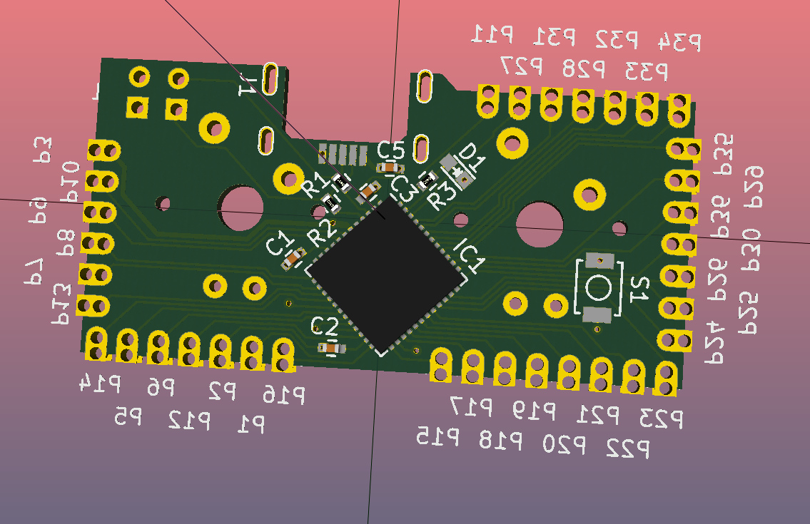
- demo5.png (321.96 KiB) Viewed 7777 times
- demo4.png (386.02 KiB) Viewed 7777 times
Just point me to a proper alps footprint and I'll add the support.
Sorry for not doing this months ago.
Posted: 14 Sep 2016, 18:03
by matt3o
pomk wrote: I mean it cannot be mounted to the bottom of two alps switches without another pcb in between.
sorry but why not? the switches are held by the plate, if the switch is a bit loose on the plate you can always hot glue it.
pomk wrote: Oh well, routed my version finally completely. I don't have the measurements for alps solder points, but there is still a lot of room to play with. It has even an almost complete ground layer. All pins on the IC have been routed.
this looks good to me, I believe the switches should be upside down though, so the LED is on top.
Posted: 14 Sep 2016, 21:13
by pomk
Agree to disagree on the LED positions? I prefer cherry caps.
The question is not about the switches staying in place, but rather the elf board. If the board cannot be soldered on the switches, as was the case in the pcb you posted, there will be nothing to keep it in place.
Posted: 15 Sep 2016, 00:24
by matt3o
Like I said I believe the LED should be on top and possibly the peninsula should be... well a real peninsula
Other than that I can't really comment on your design I wish more experienced people could chime in. If it works... I like it