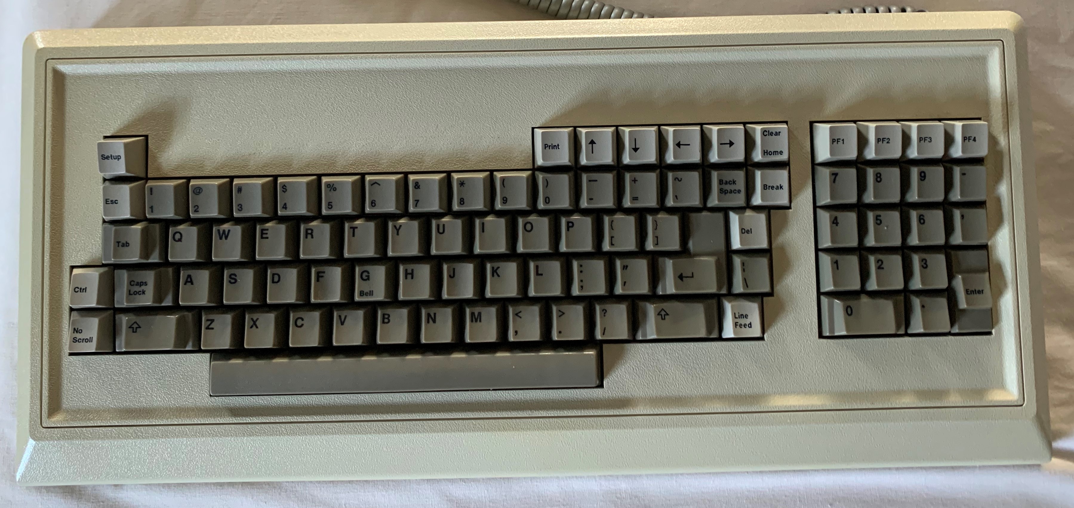
The Qume (ITT subsidary) QVT-101 was a low-cost green screen ASCII (dumb) terminal from the mid-80's. It competed against the likes of the ADM-3A in the sub-$500 market. For ANSI (smart) terminals, in particular with VT100 compatibility, there were other higher-end QVT models. I believe these capabilities eventually merged down with the QVT-103.
- QVT-101-case.jpg (1.32 MiB) Viewed 4493 times
Even though it could not emulate a VT100, there were a number of things about the keyboard copied from the VT100, sometimes for no obvious (to me) gain. Most apparent is the layout, which other than a smaller Setup key and adding a couple of keys around the arrows, is the same. There are, of course, no LEDs, to keep it cheaper.
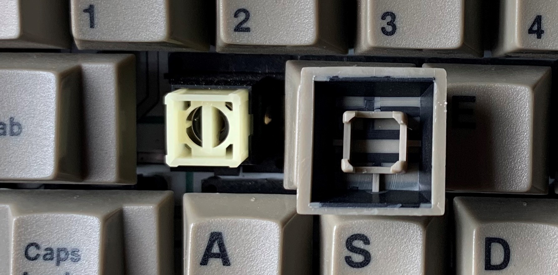
It has membrane switches with spring sliders. Somewhat surprisingly, most of the caps are thin double-shot. I believe that further cost cutting in the QVT-102 eliminated these for printed caps.
- QVT-101-keycap.jpg (354.37 KiB) Viewed 4493 times
I doubt that they were ever very good, but a little bit of corrosion on the PCB below the membrane now makes the switches very unreliable. Cleaning would mean removing the slider/spring housings, which are held in by rivets. While it might be possible to remove these without damage, I am not sure it's worth it.
The pinout and basics of the signaling are in
kbdbabel. The schematic is in
Bitsavers. The schematic for the QVT-102 is also
there and they are evidently more or less the same.
There are also some
detailed pictures of a disassembled QVT-102. Here again, the physical circuit layout is very similar.
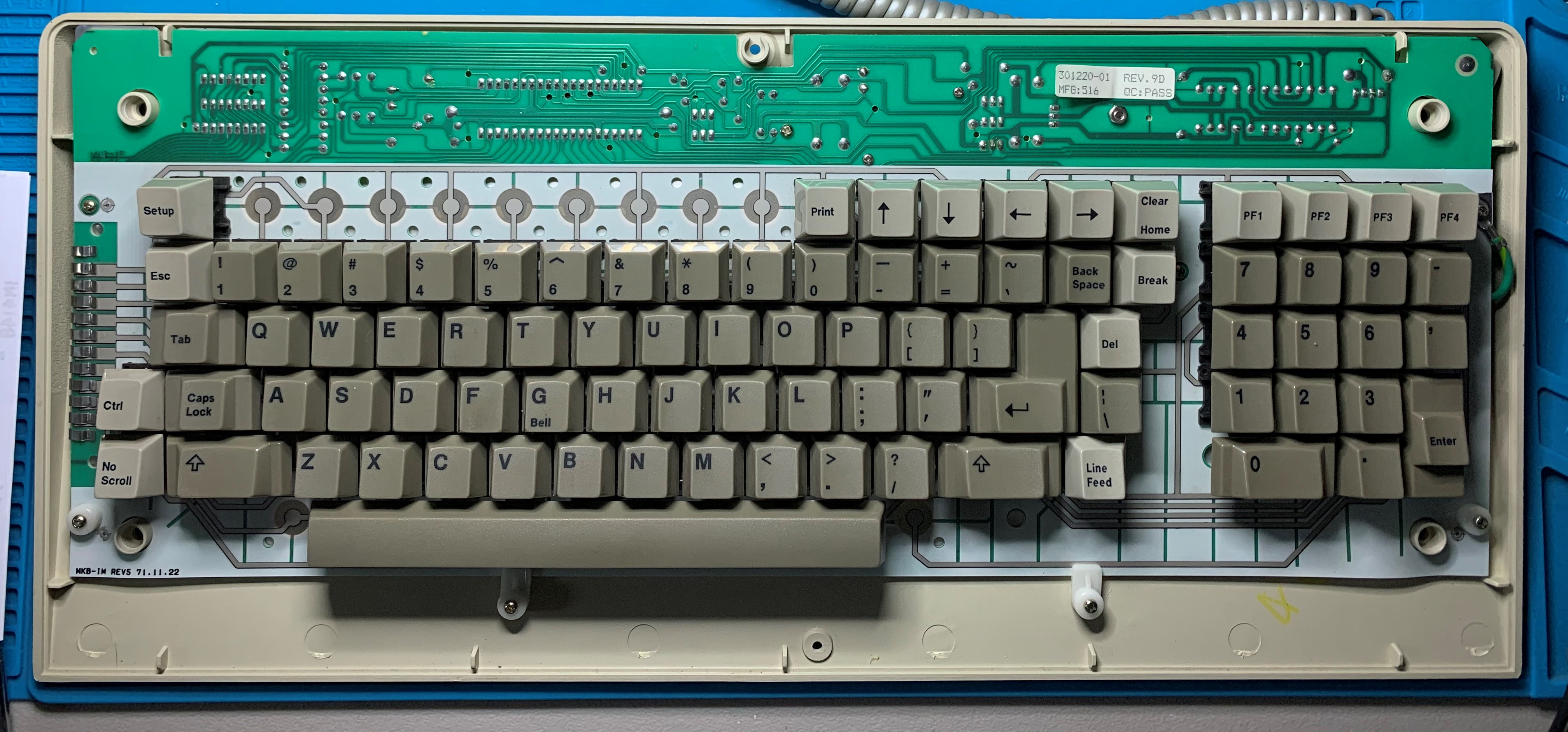
- QVT-101-top.jpg (1.45 MiB) Viewed 4493 times
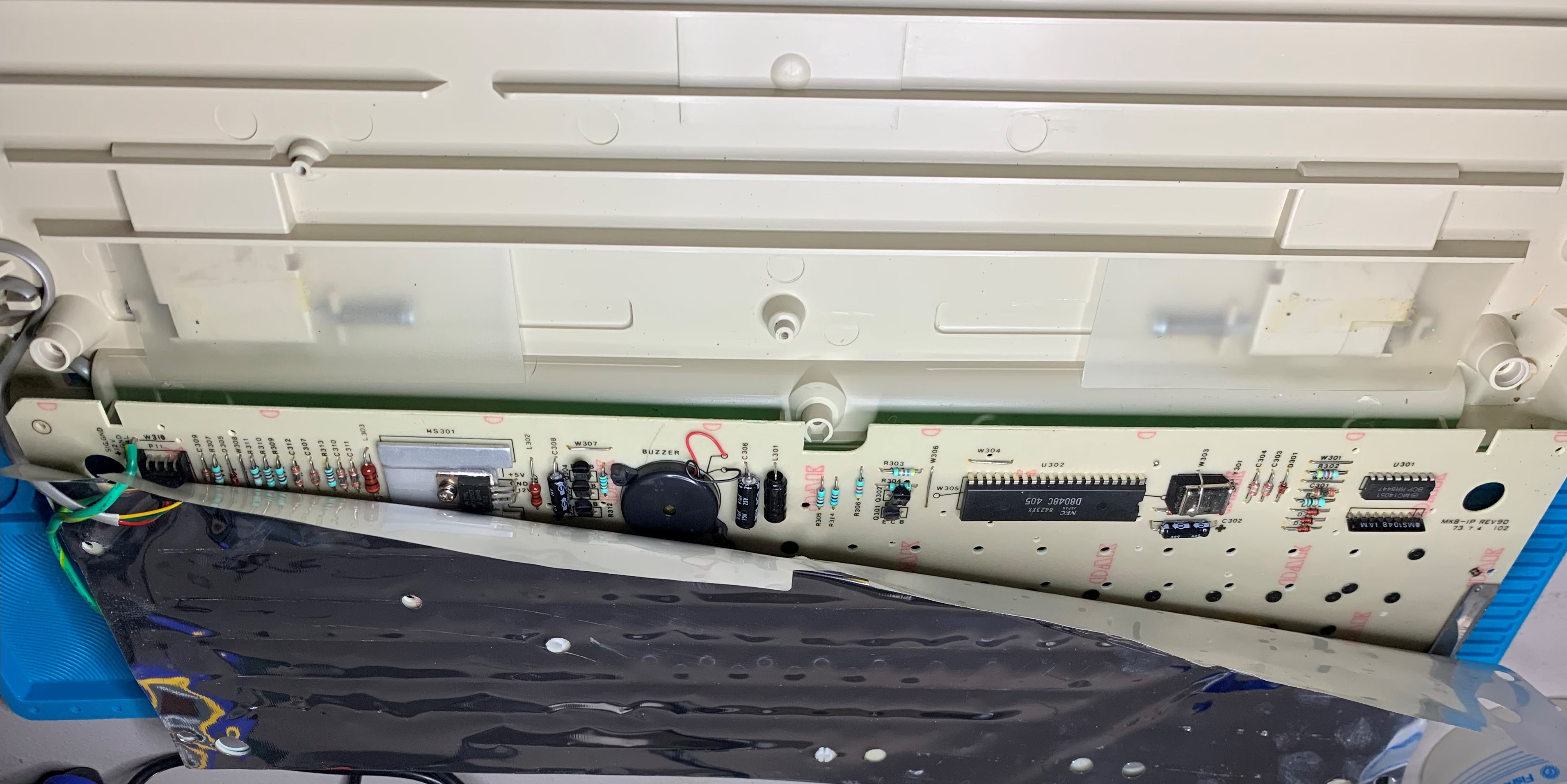
- QVT-101-bottom.jpg (994.54 KiB) Viewed 4493 times
The
QVT-102 firmware is also there. Using this, it is possible to confirm the timing and the details of the protocol encoding. For example, here are the most important parts of scanning and transmitting.
Code: Select all
00A3							L00A3:
00A3 : FE			    " "		[1]		mov	a,r6
00A4							L00A4:
00A4 : 88 70			    " p"	[2]		orl	bus,#070H
00A6							L00A6:
00A6 : D2 AA			    "  "	[2]		jb6	L00AA
00A8 : 98 BF			    "  "	[2]		anl	bus,#0BFH
00AA							L00AA:
00AA : B2 AE			    "  "	[2]		jb5	L00AE
00AC : 98 DF			    "  "	[2]		anl	bus,#0DFH
00AE							L00AE:
00AE : 92 B2			    "  "	[2]		jb4	L00B2
00B0 : 98 EF			    "  "	[2]		anl	bus,#0EFH
00B2							L00B2:
00B2 : 93			    " "		[2]		retr
							;
00B3							L00B3:
00B3 : 23 01			    "# "	[2]		mov	a,#001H
00B5							L00B5:
00B5 : D3 80			    "  "	[2]		xrl	a,#080H
00B7 : 35			    "5"		[1]		dis	tcnti
00B8 : 15			    " "		[1]		dis	i
00B9 : 9A 7F			    "  "	[2]		anl	p2,#07FH
00BB : B9 1F			    "  "	[2]		mov	r1,#01FH
00BD							L00BD:
00BD : E9 BD			    "  "	[2]		djnz	r1,L00BD
00BF : B9 0A			    "  "	[2]		mov	r1,#00AH
00C1 : 97			    " "		[1]		clr	c
00C2 : A7			    " "		[1]		cpl	c
00C3							L00C3:
00C3 : 00			    " "		[1]		nop
00C4 : 00			    " "		[1]		nop
00C5 : 67			    "g"		[1]		rrc	a
00C6 : 3A			    ":"		[2]		outl	p2,a
00C7 : E9 C3			    "  "	[2]		djnz	r1,L00C3
00C9 : 25			    "%"		[1]		en	tcnti
00CA							L00CA:
00CA : 16 07			    "  "	[2]		jtf	L0007
00CC : 05			    " "		[1]		en	i
00CD : 93			    " "		[2]		retr
							;
00CE							L00CE:
00CE : 89 FF			    "  "	[2]		orl	p1,#0FFH
00D0 : 8A FF			    "  "	[2]		orl	p2,#0FFH
00D2 : FE			    " "		[1]		mov	a,r6
00D3 : 53 07			    "S "	[2]		anl	a,#007H
00D5 : E3			    " "		[2]		movp3	a,@a
00D6 : 2E			    "."		[1]		xch	a,r6
00D7 : 72 DD			    "r "	[2]		jb3	L00DD
00D9 : 2E			    "."		[1]		xch	a,r6
00DA : 39			    "9"		[2]		outl	p1,a
00DB : 04 E0			    "  "	[2]		jmp	L00E0
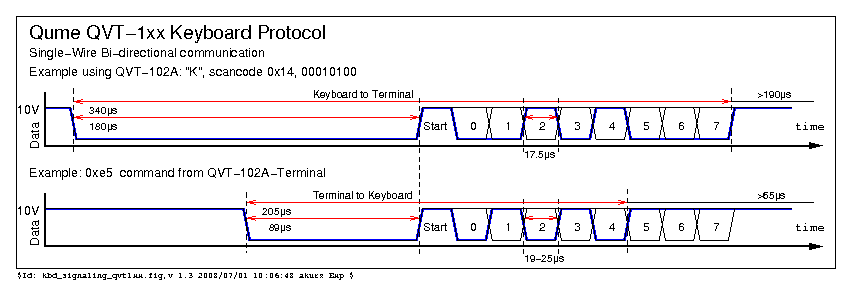
- B5 sends a byte; the C3 transmit loop is 7 cycles long. At 6MHz, that gives a width of 17.5µs, or around 57kbps.
- A4 loads the row number from the high nibble of R6 into the 4015 mux.
- CE sets the column number from the low nibble of R6 into P1 and P2.
The connector on the keyboard is a 4P4C RJ jack. The coiled cable that comes with the keyboard is crossover, like on a telephone handset, so the pins need to be reversed.
The signals are GND, +12V, PE, and SIG. Other than the connector type and the chassis ground, this is reminiscent of the VT100, with +12V power required and not just for a regulator, because the bidirectional data line is idle high at around 10-12V.
Although there are no LEDs, terminal to keyboard is needed to control the buzzer.
The
circuit for combining the input and output signals is less clever than the DEC one without aiming for simultaneity: an open-collector inverter for pulling down output and a PNP transistor to compare input voltage and drive another inverter. A converter can just borrow this to connect two GPIOs.
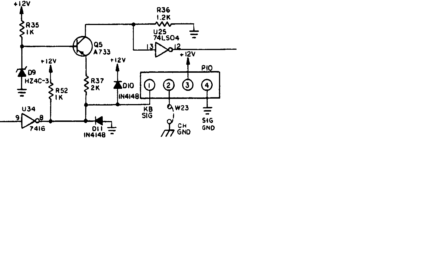
- QVT-102-signal.png (29.72 KiB) Viewed 4493 times
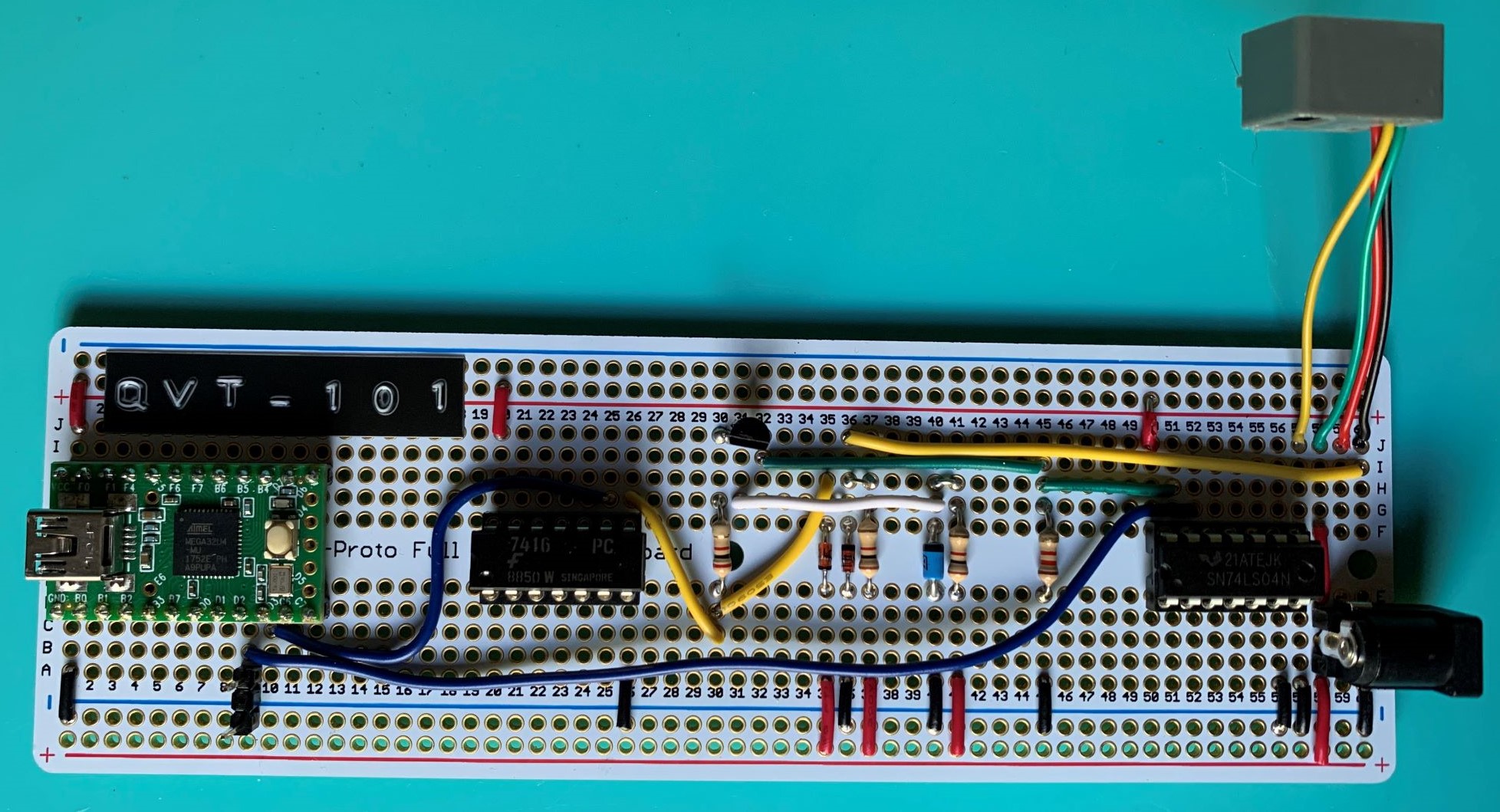
- QVT-101-converter.jpg (480.73 KiB) Viewed 4493 times
Note how the RJ colors are reversed to match with the cable's transposition.
These (inverted) TTL level signals are also compatible with a logic analyzer and a simple Sigrok decoder for the protocol confirms the serial encoding.
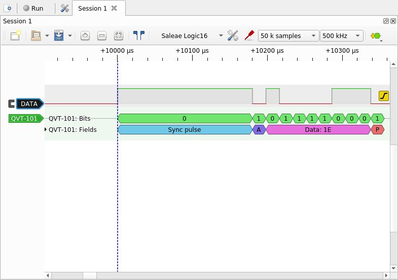
- QVT-101-A.png (36.09 KiB) Viewed 4493 times
The long pulse to grab the bus as the start means that the start bit proper has the same polarity as idle, so it is not possible to use a UART to do this encoding/decoding. It has to be bit-banged.
As noted in the disassembly above, the scan code is just four bits of column and three bits of row right off the schematic.
But note how the schematic calls out that the matrix is VT100 compatible. This is true; compare with the
VT100 Technical Manual. Here is where I am not sure what the point is. The scan codes aren't the same, and are, in any case, internal to the keyboard. Is it just that the two kinds of terminals then have the same ghosting behavior, since there are no diodes?
A normal key press consists of two bytes. The first is the scan code, which cannot have the eighth bit set. The second always has 80 set and gives the state of the Shift (10) and Ctrl (20) keys. The low bits of this second byte distinguish initial key press (4) from auto-repeat.
The remaining special cases are 81 at power-on and 82 for Caps Lock press. These do not have a preceding scan code byte.
There are no up transitions. The two shift keys cannot be distinguished. It is not possible to enlist other keys are shifts. So, all in all, implementation of a USB keyboard has to be pretty minimal.
